68kMLA Classic Interface
This is a version of the 68kMLA forums for viewing on your favorite old mac. Visitors on modern platforms may prefer the main site.
| Click here to select a new forum. | |
| Calling anyone with a working Color Classic and a Multimeter | |
| Posted by: willmurray461 on 2022-08-15 16:15:08 I just recapped my color classic, but it still doesn't work. After reading an older post here, I noticed that Y1 was disconnected from C56 due to a bad via. However, I had a little soldering accident and destroyed one of the traces/vias coming off of C56. Does anyone have a working color classic motherboard and a multimeter that they could use to probe out where that trace goes so I can make a bodge wire? | |
| Posted by: 360alaska on 2022-08-15 16:26:15 Both of my Color Classics have 575 Boards, but I offer you a community sourced schematic: https://drive.google.com/file/d/1gB029UsD3JoRYssmSmX2rUhhPEoVPhed/view?usp=sharing | |
| Posted by: willmurray461 on 2022-08-15 16:31:22 I've already looked at the Bomarc schematics, and either they are for a different board revision, are erroneous, or I'm not reading them right. It says that the left leg of Y1 connects to C36 (it should be C56) and R36. However, it makes no mention of the third trace I'm trying to figure out... | |
| Posted by: bibilit on 2022-08-16 00:39:02 i will have a look this evening | |
| Posted by: willmurray461 on 2022-08-16 06:08:17 I was following this guide. The trace I'm referring to is the one that goes down and to the right off of the left side of C56 in the second picture. | |
| Posted by: bibilit on 2022-08-16 06:58:15 in other words, you want to know where the left pad of C56 goes ? probably to the trace you see just underneath... but i will check anyway IIRC the right pad of C56 goes to ground. | |
| Posted by: willmurray461 on 2022-08-16 07:01:25 I broke off the circular pad at the end of the trace underneath, and it doesn’t seem to go all the way through the board like a normal via so I don’t know where that pad goes. | |
| Posted by: SuperSVGA on 2022-08-16 08:24:00 It definitely appears to go to ground on my board. It does not appear to be a blind via either. I can see the two vias below C56 match up with the two under Y1. The blind vias appear to be plated/plugged. | |
| Posted by: willmurray461 on 2022-08-16 08:27:57 Just to be clear, I am referring to the pad pictured here. Are you sure it connects to ground? 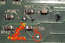 | |
| Posted by: SuperSVGA on 2022-08-16 08:37:33 Sorry, I thought we were talking about the right side connection of C56. That one is a blind via, so it's hard to tell, but I'm guessing it goes to R37 since there doesn't seem to be anything else connecting it. | |
| Posted by: willmurray461 on 2022-08-16 09:58:49 That pin of the oscillator is already connected to R37 via another via… My hope is that you’d just be able to blindly probe around with a multimeter in continuity mode to see if you can find a beep… | |
| Posted by: bibilit on 2022-08-16 10:40:23 Ok, so your pad is connected to the the left pad of C56. The same pad goes on the other side of the board, and is connected to right pad of Y1. | |
| Posted by: willmurray461 on 2022-08-16 10:48:37 I already got that part down. I’m actually trying to figure out the same in reverse, i.e. aftet leaving Y1 and going to the left side of c56, where does it go after disappearing into the blind via? | |
| Posted by: mg.man on 2022-08-16 11:11:34 On my (working) CC I 'board, all these points have continuity... 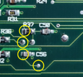 Hope this helps. | |
Posted by: SuperSVGA on 2022-08-16 11:26:16That pin of the oscillator is already connected to R37 via another via…Right, it is likely connected from the blind via to the via you can see above R37. I don't see any reason why it would go anywhere else. | |
| Posted by: willmurray461 on 2022-08-16 13:04:48 I'm pretty sure the via above R37 connects through on the other side directly to one of the pins of the oscillator. It also still has continuity on my machine, even though the blind via is gone, so I'm assuming the blind via goes elsewhere. Honestly, I'm beginning to think that blind via might not go anywhere. I couldn't find anything by trying to dig around the trace, and its possible that another via elsewhere was destroyed by leaky capacitors and is the cause of my problems. Either way, if we can't fix the problem that's fine as I was planning on turning this machine into a TAKKY anyway. | |
| Posted by: SuperSVGA on 2022-08-16 13:49:20 I can't see anything missing from the schematic though. 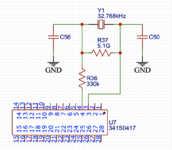 You have:
| |
| Posted by: willmurray461 on 2022-08-16 14:13:39 That's why I'm confused. Why have a trace+via that doesn't go anywhere? At first, I just thought it was possibly due to the fact that the schematics were reverse engineered, and thus possibly incomplete. However, it doesn't seem that way... | |
| Posted by: SuperSVGA on 2022-08-16 14:27:31 It might actually just be a test pad rather than a via. I fiddled with mine a bit, and it seems more like a flat disc that just lifts right off the board. | |
| Posted by: willmurray461 on 2022-08-16 14:29:48 That’s pretty much what I experienced. Guess that settles it, it’s probably a test pad. I guess I need to look around for more corroded vias then near the other capacitors then. | |
| 1 |