68kMLA Classic Interface
This is a version of the 68kMLA forums for viewing on your favorite old mac. Visitors on modern platforms may prefer the main site.
| Click here to select a new forum. | |
| SE/30 DiiMO accelerator cloning | |
Posted by: Bolle on 2020-03-04 10:14:02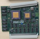 I figured that it might be worth sharing this to maybe spark somebodies interest in getting the GAL logic dumbed down into something more modern to drastically reduce the size of this thing to free space for additional PDS cards. So far I happen to have figured out the schematics: View attachment DiiMOSE30.png And I also extracted the GAL code: ;$GALMODE MEDIUM
chip U1 GAL16V8
i1=1 i2=2 i3=3 i4=4 i5=5 i6=6 i7=7 i8=8 i9=9 GND=10 /i11=11 o12=12
f13=13 f14=14 o15=15 f16=16 f17=17 o18=18 o19=19 VCC=20
@ues 0000000000000000
@ptd unused
equations
/o19 = /i2 * f14 * /f13 * /i11
o19.oe = vcc
/o18 = /i4
+ /i1 * /i6
+ /i2 * i1 * i3 * i5 * /i7 * i8 * i9 * i11
+ /i2 * i1 * i3 * i5 * i7 * /i8 * i9 * i11
+ /i2 * i1 * i3 * i5 * /i7 * /f14 * i8 * /f13 * i9
+ /i2 * i1 * i3 * i5 * i7 * /f14 * /i8 * /f13 * i9
o18.oe = vcc
/f17 = /i2 * i1 * i3 * i5 * /i7 * i8 * i9 * i11
+ /i2 * i1 * i3 * i5 * i7 * /i8 * i9 * i11
+ /i2 * i1 * i3 * i5 * /i7 * /f14 * i8 * /f13 * i9
+ /i2 * i1 * i3 * i5 * i7 * /f14 * /i8 * /f13 * i9
f17.oe = vcc
f16 = gnd
f16.oe = gnd
/o15 = /f16
o15.oe = f17
f14 = gnd
f14.oe = gnd
f13 = gnd
f13.oe = gnd
/o12 = /i2 * i1 * i3 * /i7 * i8 * i9 * i11
+ /i2 * i1 * i3 * i7 * /i8 * i9 * i11
+ /i2 * i1 * i3 * /i7 * /f14 * i8 * /f13 * i9
+ /i2 * i1 * i3 * i7 * /f14 * /i8 * /f13 * i9
o12.oe = vcc;$GALMODE REGISTERED
chip U2 GAL16V8
CLK=1 i2=2 i3=3 i4=4 i5=5 i6=6 i7=7 i8=8 i9=9 GND=10 /OE=11 rf12=12
rf13=13 rf14=14 rf15=15 rf16=16 rf17=17 rf18=18 o19=19 VCC=20
@ues 0000000000000000
@ptd unused
equations
/o19 = /i2
o19.oe = vcc
rf18 := rf18 * rf17 * rf14
+ i3 * i4 * rf17 * rf14 * i9
rf18.oe = OE
/rf17 := rf18 * rf17 * /i9
+ rf18 * rf17 * /rf14 * /i8
+ rf18 * rf17 * /i7 * /rf14
+ /i3 * /i4 * /i5 * /i6
rf17.oe = OE
/rf16 := /rf16 * /i6
+ rf18 * i5 * /i6 * i7 * /rf14 * i8 * /rf12
rf16.oe = OE
/rf15 := /i6 * /rf15
+ rf18 * i5 * /i6 * i7 * /rf14 * i8 * /rf13
rf15.oe = OE
rf14 := /rf18
+ rf13 * rf12
+ /i3 * i7 * i8 * rf12
+ /i4 * i7 * i8 * rf13
+ /i3 * /i4 * i7 * i8
rf14.oe = OE
/rf13 := /i3 * rf18
+ rf18 * /rf13
rf13.oe = OE
/rf12 := rf18 * /i4
+ rf18 * /rf12
rf12.oe = OE;$GALMODE REGISTERED
chip U3 GAL16V8
CLK=1 i2=2 i3=3 i4=4 i5=5 i6=6 i7=7 i8=8 i9=9 GND=10 /OE=11 f12=12
rf13=13 rf14=14 f15=15 f16=16 rf17=17 rf18=18 f19=19 VCC=20
@ues 0000000000000000
@ptd unused
equations
f19 = gnd
f19.oe = gnd
/rf18 := i2 * i3 * /rf18 * i4 * i9
+ i2 * i3 * i4 * rf17 * f16 * /i6 * f15 * /i7 * rf14 * i9 * f12
+ i2 * i3 * i4 * rf17 * i5 * f16 * /i6 * f15 * rf14 * i9 * f12
+ i2 * f19 * i3 * i4 * rf17 * f16 * f15 * rf14 * /i8 * rf13 * i9
rf18.oe = OE
/rf17 := /i2 * rf17 * rf14
+ f19 * rf18 * /i5 * /i6 * /i7 * rf14
rf17.oe = OE
/f16 = /i4 * /i6
f16.oe = f12
/f15 = /i3 * /i6
f15.oe = f12
/rf14 := /rf18 * /rf14 * i9
+ i2 * f19 * /rf18 * /i5 * /i7 * i9
rf14.oe = OE
rf13 := /rf13 * /i9
+ i2 * i3 * rf18 * i4 * rf17 * f16 * /i6 * f15 * rf14 * f12
rf13.oe = OE
f12 = gnd
f12.oe = gnd;$GALMODE REGISTERED
chip U4 GAL16V8
CLK=1 i2=2 i3=3 i5=5 i6=6 i7=7 i8=8 GND=10 /OE=11 o12=12 rf13=13
rf14=14 rf15=15 rf16=16 rf17=17 rf18=18 f19=19 VCC=20
@ues 0000000000000000
@ptd unused
equations
/f19 = /i3 * /i6 * /rf13
+ /i5 * /i6 * /rf13
+ /f19 * /i6
f19.oe = vcc
rf18 := f19 * rf18 * /rf16 * /i6 * /i7 * rf13
+ f19 * rf18 * /i6 * /rf15 * /i7 * rf13
+ f19 * rf18 * /rf17 * /i6 * /i7 * rf13
+ f19 * /rf18 * rf17 * rf16 * /i6 * rf15 * /i7 * rf14 * rf13
+ f19 * rf18 * /i6 * /i7 * /rf14 * rf13
rf18.oe = OE
rf17 := f19 * rf17 * /i6 * /rf15 * /i7 * rf13
+ f19 * rf17 * /rf16 * /i6 * /i7 * rf13
+ f19 * /rf17 * rf16 * /i6 * rf15 * /i7 * rf14 * rf13
+ f19 * rf17 * /i6 * /i7 * /rf14 * rf13
rf17.oe = OE
rf16 := f19 * rf16 * /i6 * /i7 * /rf14 * rf13
+ f19 * rf16 * /i6 * /rf15 * /i7 * rf13
+ f19 * /rf16 * /i6 * rf15 * rf14 * rf13
+ rf15 * i7 * rf14
rf16.oe = OE
rf15 := i5 * rf15 * /i8
+ /i5 * /rf15 * rf14 * /i8
+ f19 * /i6 * /rf15 * /i7 * rf14 * rf13
+ f19 * /i6 * rf15 * /i7 * /rf14 * rf13
+ rf15 * /rf14 * /i8
rf15.oe = OE
rf14 := /i5 * /rf14 * /i8
+ f19 * /i6 * /i7 * /rf14 * rf13
+ i5 * rf14 * /i8
rf14.oe = OE
/rf13 := i2 * i3 * i5 * /rf13
+ f19 * rf18 * rf17 * rf16 * /i6 * rf15 * /i7 * rf14
+ i2 * f19 * i3 * i5 * /rf16 * /i6 * /rf15 * i7 * /rf14
+ i2 * /i8 * /rf13
rf13.oe = OE
o12 = gnd
o12.oe = gnd;$GALMODE REGISTERED
chip U5 GAL16V8
CLK=1 i2=2 i3=3 i4=4 i5=5 i6=6 i7=7 i8=8 i9=9 GND=10 /OE=11 f12=12
f13=13 rf14=14 rf15=15 rf16=16 rf17=17 o18=18 o19=19 VCC=20
@ues 0000000000000000
@ptd unused
equations
/o19 = /i3
o19.oe = vcc
o18 = i3 * i5 * i9
o18.oe = vcc
/rf17 := /i2 * /rf17 * rf15
+ /i2 * rf17 * /rf15
rf17.oe = OE
/rf16 := /i2 * rf17 * /rf16
+ /i2 * /rf17 * rf16 * /rf15
+ /i2 * /rf16 * rf15
rf16.oe = OE
/rf15 := /i2 * /i4 * /rf14 * i8
rf15.oe = OE
/rf14 := /i2 * i3
rf14.oe = OE
/f13 = i2 * rf14 * /f12
+ i5 * rf14 * /f13
+ /i2 * /f13
f13.oe = vcc
/f12 = /i6 * /i7 * /rf14
+ /rf14 * /f12
f12.oe = vcc;$GALMODE MEDIUM
chip U6 GAL16V8
i1=1 i2=2 i3=3 i4=4 i5=5 i6=6 i7=7 i8=8 i9=9 GND=10 /i11=11 o12=12
f13=13 f14=14 f15=15 f16=16 f17=17 o18=18 o19=19 VCC=20
@ues 0000000000000000
@ptd unused
equations
o19 = i5 * i6 * i9
+ /i5 * /i8 * /i9
+ /i5 * /i6 * i8 * i9
+ i5 * /i6 * i8 * /i9
+ i5 * /i8 * i9
+ /i5 * i6 * /i9
o19.oe = vcc
o18 = i6 * i8
+ /i6 * /i8
o18.oe = vcc
/f17 = /i2 * /f13
+ /f17 * /f14 * f13
+ /i2 * /f14
f17.oe = vcc
f16 = gnd
f16.oe = gnd
f15 = i4 * f16 * f15
+ /i2 * i1 * /f16 * i7 * /f13 * i11
+ i2 * i4 * f15
+ i4 * f15 * f13
+ i4 * f15 * /i11
+ i4 * f15 * /i7
f15.oe = vcc
/f14 = /i2 * /i3
f14.oe = /i3
f13 = gnd
f13.oe = gnd
o12 = i3 * /f13
o12.oe = vcc;$GALMODE SMALL
chip U7 GAL16V8
i1=1 i2=2 i3=3 i4=4 i5=5 i6=6 i7=7 i8=8 i9=9 GND=10 /i11=11 o12=12
f13=13 f14=14 o15=15 o16=16 o17=17 o18=18 o19=19 VCC=20
@ues 0000000000000000
@ptd unused
equations
/o19 = /i2 * /i3 * f14 * /i8 * /i9 * i11
+ /i2 * f13
/o18 = /i2 * /i3 * f14 * /i8 * i9 * i11
+ /i2 * /i3 * f14 * i7 * /i8 * i11
+ /i2 * /i3 * /i6 * f14 * /i8 * i11
+ /i2 * f13
/o17 = /i2 * /i3 * f14 * /i8 * /i9 * /i11
+ /i2 * f13
+ /i2 * /i3 * f14 * i7 * /i8 * i9 * i11
+ /i2 * /i3 * /i6 * f14 * /i7 * /i8 * i11
+ /i2 * /i3 * i6 * f14 * i7 * /i8 * i11
/o16 = /i2 * /i3 * f14 * /i8 * i9 * /i11
+ /i2 * /i3 * /i6 * f14 * /i7 * /i8
+ /i2 * /i3 * f14 * i7 * /i8 * /i11
+ /i2 * /i3 * i6 * f14 * i7 * /i8 * i9
+ /i2 * f13
f13 = /i1 * /i4 * /i5
/o12 = /i2 * f13;$GALMODE MEDIUM
chip U8 GAL16V8
i1=1 i4=4 i5=5 i6=6 i7=7 i8=8 i9=9 GND=10 /i11=11 o12=12 o13=13
f14=14 f15=15 f16=16 f17=17 f18=18 o19=19 VCC=20
@ues ffffffffffffffff
equations
o19 = /i1 * i4 * f17 * i8 * i9
+ /i1 * i4 * f15 * i8 * /i9
+ /i1 * i4 * f16 * /i8 * i9
+ /i1 * i4 * f14 * /i8 * /i9
o19.oe = vcc
f18 = gnd
f18.oe = gnd
f17 = i8 * i9
+ i11
+ i4 * f17
f17.oe = /i1 * i7
f16 = /i8 * i9
+ i11
+ i4 * f16
f16.oe = /i1 * i7
f15 = i8 * /i9
+ i11
+ i4 * f15
f15.oe = /i1 * i7
f14 = /i8 * /i9
+ i11
+ i4 * f14
f14.oe = /i1 * i7
o13 = i4 * f17 * i8 * i9
+ i4 * f15 * i8 * /i9
+ i4 * f16 * /i8 * i9
+ i4 * f14 * /i8 * /i9
+ i1 * i6
o13.oe = /i5
o12 = f18 * i4 * f17 * i8 * i9
+ f18 * i4 * f15 * i8 * /i9
+ f18 * i4 * f16 * /i8 * i9
+ f18 * i4 * f14 * /i8 * /i9
+ i1 * f18 * i6
+ f18 * i5
o12.oe = vcc;$GALMODE REGISTERED
chip U9 GAL16V8
CLK=1 i2=2 i3=3 i4=4 i5=5 i6=6 i7=7 i8=8 i9=9 GND=10 /OE=11 o12=12
f13=13 f14=14 f15=15 o16=16 rf17=17 f18=18 o19=19 VCC=20
@ues 0000000000000000
@ptd unused
equations
o19 = /i2
o19.oe = vcc
/f18 = /i2 * /i9
+ i2 * /f18
f18.oe = i8
/rf17 := /i3 * /f14
+ /i4 * /f14
rf17.oe = OE
o16 = /f18 * /i5
+ /i5 * /i7
o16.oe = vcc
/f15 = /i2 * i5 * /i9
+ /i2 * /f13 * /i9
+ i2 * /f15
f15.oe = i8
f14 = /i4 * f14
+ i2 * /i6
+ /i3 * f14
+ /rf17 * i9
f14.oe = vcc
/f13 = i2 * /f18 * /i5 * /i9
+ /f13 * /i9
f13.oe = vcc
o12 = i3 * i4
o12.oe = vcc;$GALMODE REGISTERED
chip U10 GAL16V8
CLK=1 i2=2 i3=3 i4=4 i5=5 i6=6 i7=7 i8=8 i9=9 GND=10 /OE=11 f12=12
f13=13 o14=14 f15=15 o16=16 f17=17 ro18=18 rf19=19 VCC=20
@ues 0000000000000000
@ptd unused
equations
/rf19 := /i2 * /rf19
+ /i2 * i4
rf19.oe = OE
/ro18 := /i3 * i4 * i5
ro18.oe = OE
f17 = gnd
f17.oe = gnd
/o16 = f17 * i6 * f15 * /i7 * /i8 * /f13 * /i9 * /f12
o16.oe = vcc
f15 = gnd
f15.oe = gnd
/o14 = i8 * /f13 * /i9 * /f12
+ i7 * i8 * /f12
o14.oe = vcc
f13 = gnd
f13.oe = gnd
f12 = gnd
f12.oe = gnd;$GALMODE MEDIUM
chip U24 GAL16V8
i1=1 i2=2 GND=10 /nc11=11 o12=12 f13=13 f14=14 f15=15 o16=16
o17=17 o18=18 o19=19 VCC=20
@ues 0000000000000000
@ptd unused
equations
o19 = gnd
o19.oe = gnd
/o18 = /f13
o18.oe = vcc
/o17 = /i1
o17.oe = vcc
/o16 = /i1
o16.oe = vcc
/f15 = /i2 * /f15
+ /i2 * /i1
f15.oe = vcc
/f14 = /f15
f14.oe = vcc
/f13 = /f14
f13.oe = vcc
o12 = gnd
o12.oe = gnd;$GALMODE MEDIUM
chip U33 GAL16V8
i1=1 i2=2 i3=3 i4=4 i5=5 i6=6 i7=7 i8=8 i9=9 GND=10 /i11=11 o12=12
f13=13 o14=14 f15=15 f16=16 f17=17 f18=18 o19=19 VCC=20
@ues 0000000000000000
@ptd unused
equations
o19 = /i6
+ i1 * i7 * /i8 * /i9
+ i11
o19.oe = vcc
f18 = gnd
f18.oe = gnd
/f17 = i2 * i3 * /f18 * /i4
+ /i3 * /f17 * /i5 * f13
+ /i3 * /f17 * /f15 * f13
+ /i3 * /i4 * /f17 * f13
f17.oe = vcc
/f16 = /f18 * /f16 * f13
+ /i3 * /f18 * f13
f16.oe = vcc
f15 = gnd
f15.oe = gnd
o14 = gnd
o14.oe = gnd
f13 = gnd
f13.oe = gnd
/o12 = /i1 * i6 * i7 * /i8 * /i9 * /i11
o12.oe = vccI also confirmed all of this is actually correct and working :evil: 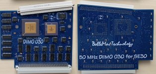 So who's up for the challenge to translate all that into something modern or come up with something better than just rebuilding the original? | |
| Posted by: trag on 2020-03-04 10:56:10 Very nice. Looking forward to following this. | |
| Posted by: olePigeon on 2020-03-04 13:46:20 Could this be used to also make an 040 upgrade? | |
Posted by: trag on 2020-03-04 14:41:57Could this be used to also make an 040 upgrade?I think he's looking at the GAL based Daystar Turbo040 card for that possibility. Although, since a limited supply of the large ASIC used on the later Turbo040 was found, it might just go in that direction, at least while the supply of ASICs holds out. | |
Posted by: mdeverhart on 2020-03-04 19:44:12So who's up for the challenge to translate all that into something modern or come up with something better than just rebuilding the original?I'll take a stab at converting the logic to Verilog that can be synthesized into a (more) modern CPLD (AFAIK, nothing truly modern is natively 5V tolerant, requiring either external level shifters or external resistors and diodes to clamp the signals for use on 3.3V IO). I don't have ton of time for projects, so it may take me a bit - if anyone with more time wants to take a stab, feel free. | |
| Posted by: trag on 2020-03-05 11:03:59 Atmel and Altera, I think, still have 5V CPLDs in production. I'm certain Atmel does. Not sure if there are any actual FPGAs out there, although the lines between them blur. | |
Posted by: mdeverhart on 2020-03-30 17:54:02I'm certain Atmel does.You’re absolutely right, Atmel does: https://www.microchip.com/design-centers/fpgas-and-plds/splds-cplds Altera discontinued theirs. Atmel got bought by Microsemi (before Microsemi got bought by Microchip), and Atmel’s FPGAs are listed on the Microsemi website. I didn’t realize that their CPLDs were on the Microchip site. I’ll need to dig through some data sheets and see if I can find a suitable device. I’ve had a little bit of time to look at this, but not a ton. Most of the logic is straightforward, but I’m trying to wrap my head around the feedback paths and the inversions/polarities on those paths. @Bolle What program did you use to dump the equations from the JED files? I’d like to try assembling and then disassembling some of my own logic to better understand some of those equations. Would you be willing to email me the JED files you extracted if I PM’d you my email address? | |
| Posted by: Bolle on 2020-03-30 23:02:36 Sure, they are not exactly a secret 😉 I use the tools that come with opaljr to assemble/disassemble jedec files. Indeed most of the stuff just makes sense after staring at it long enough but the feedbacks and some of the register stuff is breaking my head. Especially if you take the different clock domains into account and how those clocks are sometimes phase shifted to each other after they are buffered and/or inverted somewhere. View attachment DiiMO_GALs.zip | |
| Posted by: mdeverhart on 2020-03-31 11:15:40 Thanks. I didn’t realize the forum SW allowed for arbitrary file attachments. I haven’t gotten to thinking about the clock buffering/shifts yet. Good times! | |
Posted by: Melkhior on 2022-01-17 09:37:19So who's up for the challenge to translate all that into something modern or come up with something better than just rebuilding the original?Have you found a solution for this ? Otherwise, I guess under the assumption "a=b" is combinatorial and "a:=b" is clocked, it should not be very hard to write an ad-hoc parser and generate a Verilog module for each GAL file. There would still be the need to connect them all as per the schematics, but the equation themselves should be OK. | |
Posted by: Bolle on 2022-01-17 09:44:22"a=b" is combinatorial and "a:=b" is clockedCorrect. Have you found a solution for this ?Nope, but I haven't actually looked into it actively either 😀 | |
| Posted by: esselfortium on 2022-01-17 09:52:32 This is amazing work. Is there any chance you might try cloning the other DiiMO cards someday? | |
Posted by: Bolle on 2022-01-17 09:57:43Is there any chance you might try cloning the other DiiMO cards someday?Which one specifically? | |
| Posted by: esselfortium on 2022-01-17 10:01:08 The one for the Mac II-series? | |
| Posted by: Bolle on 2022-01-17 10:08:20 It's the same as the SE/30 one, just a different form factor: 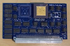 Never could get it to work reliably in the IIci though due to some (I suppose) timing issues. It was fine in IIcx and II though as far as my testing went. | |
| Posted by: esselfortium on 2022-01-17 10:12:50 Interesting... How difficult would it be to make it in that form factor? I have a II. | |
| Posted by: Bolle on 2022-01-17 10:17:17 Look at it again a little closer, that's already a remake 😉 Problem for the II is that you also need an adapter for that. I only have a Daystar adapter for my Mac II and while it runs the DiiMO just fine as it does all the PowerCaches and Turbo040s I could throw at it I am having trouble figuring out that last PAL that's on the adapter to get it cloned. So the card itself is not going to be of much use right now if you plan to run it in a Mac II. | |
Posted by: Melkhior on 2022-01-17 10:20:45Nope, but I haven't actually looked into it actively either 😀Would outputing something like that be useful? ISE seems OK with it for a XC9536XL (they are 3.3V but 5V-tolerant). module GAL16V8_U3 (
input CLK,
input i2,
input i3,
input i4,
input i5,
input i6,
input i7,
input i8,
input i9,
input OE_n,
input f12,
inout rf13,
inout rf14,
inout f15,
inout f16,
inout rf17,
inout rf18,
input f19
);
reg rf13_reg = 'b0;
reg rf14_reg = 'b0;
reg rf17_reg = 'b0;
reg rf18_reg = 'b0;
// f19 OE signal is grounded
always @(posedge clk) begin
rf18_reg <= ~((((((((i2 & i3) & (~rf18)) & i4) & i9) | ((((((((((i2 & i3) & i4) & rf17) & f16) & (~i6)) & f15) & (~i7)) & rf14) & i9) & f12)) | ((((((((((i2 & i3) & i4) & rf17) & i5) & f16) & (~i6)) & f15) & rf14) & i9) & f12)) | ((((((((((i2 & f19) & i3) & i4) & rf17) & f16) & f15) & rf14) & (~i8)) & rf13) & i9)));
end
assign rf18 = (~(OE_n)) ? rf18_reg : 'bZ;
always @(posedge clk) begin
rf17_reg <= ~(((((~i2) & rf17) & rf14) | (((((f19 & rf18) & (~i5)) & (~i6)) & (~i7)) & rf14)));
end
assign rf17 = (~(OE_n)) ? rf17_reg : 'bZ;
assign f16 = (f12) ? ~(((~i4) & (~i6))) : 'bZ;
assign f15 = (f12) ? ~(((~i3) & (~i6))) : 'bZ;
always @(posedge clk) begin
rf14_reg <= ~(((((~rf18) & (~rf14)) & i9) | (((((i2 & f19) & (~rf18)) & (~i5)) & (~i7)) & i9)));
end
assign rf14 = (~(OE_n)) ? rf14_reg : 'bZ;
always @(posedge clk) begin
rf13_reg <= (((~rf13) & (~i9)) | (((((((((i2 & i3) & rf18) & i4) & rf17) & f16) & (~i6)) & f15) & rf14) & f12));
end
assign rf13 = (~(OE_n)) ? rf13_reg : 'bZ;
// f12 OE signal is grounded
endmodule // GAL16V8_U3Edit: the large number of useless parenthesis is a side-effect of just parsing/unparsing. | |
Posted by: Melkhior on 2022-01-17 10:30:02Which one specifically?From my side, I wonder if we can leverage existing designs to create a 'modern' cache card for the IIci and/or other II-machines with PDS. With a lot of cache, as fast SRAMs are significantly cheaper now than they were then. And I assume no hard-to-find / vintage chips would be needed. | |
| Posted by: mdeverhart on 2022-01-17 12:48:20 I started hand translating some of the simpler GALs, and did some experiments with the Lattice SW and the PAL disassembly tools to make sure I understood how it was transforming them. I was hoping to be able to run my Verilog back through the Lattice SW, and then decompile the JED output to equations to check my work, but unfortunately the synthesis engine was making different optimizations than the original (presumably) hand-optimized equations. The more I looked at it, and based on some of Bolle’s other comments, I decided that the hard part would be getting similar propagation delay in a modern CPLD. I think you’d need to calculate the propagation delay through the GAL circuit, and add appropriate delay logic in the CPLD. It seems like a solvable problem (CPLDs usually document the delay per gate), but not an easy one. Alas, I haven’t had much time for projects and have others on my list, and haven’t gotten back to this one. | |
| 1 > |