68kMLA Classic Interface
This is a version of the 68kMLA forums for viewing on your favorite old mac. Visitors on modern platforms may prefer the main site.
| Click here to select a new forum. | |
| Oscilloscope 101 - Probing the bus for activity | |
| Posted by: uniserver on 2013-01-08 09:46:31 I have a dead LC-1 board and a LC-III. Also, I have an oscilloscope, I think its an TEK one in the garage, I would like to start this thread to help people that never used one, to maybe get a couple pointers Its been years and years since i'v touched one. In a NO Bong / No Videro situation, obviously you want to recap, first thing. However if that doesn't help, then ... I remember reading in another thread that you first check the bus lines for activity, can someone provide some pictures or some posts to help with this? Thank you very much ahead of time. | |
| Posted by: uniserver on 2013-01-08 10:50:11 both of these boards suffered a massive Pram battery explosion. | |
| Posted by: James1095 on 2013-01-09 12:54:56 A scope is unlikely to tell the novice much, it will show you what is there, but unless it's a DSO that can capture and hold a waveform, looking at a digital line will just look like a bunch of noise. A multimeter is a more appropriate tool for the job. Check the power supply voltages, check the reset line on the CPU, if that all looks good, *then* is a good time to pull out the scope and have a look at the clock generator. | |
| Posted by: uniserver on 2013-01-09 22:22:45 Thanks for the info, i am having issues finding pinouts, but I did come across this: 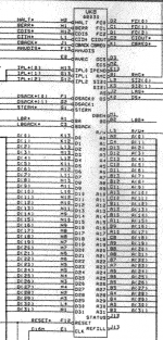 Pinout's are not exactly clear, and the drawing of the 68030 CPU is not square, Looks more like the 68000, oh well. | |
| Posted by: James1095 on 2013-01-15 12:59:48 In schematic drawings, it's common for representations of parts to be laid out logically rather than to mimic the physical layout of the part. For example all the data bus pins might be grouped together in order, all the address bus pins in another group, the power and ground pins in another group, etc while on the physical chip they may be laid out completely differently. If the schematic had the pins laid out to match the physical parts, the wiring would be a rats nest that would be a nightmare to follow. This also allows for a single schematic symbol to represent multiple different package types for the IC. The schematic is a visual representation of how the circuit is wired up together, while the pin numbers are provided so you can find the physical pin on the chip that corresponds to the schematic. | |
| 1 |