68kMLA Classic Interface
This is a version of the 68kMLA forums for viewing on your favorite old mac. Visitors on modern platforms may prefer the main site.
| Click here to select a new forum. | |
| Apple Techstep I have almost all of the ROMs here and some info! | |
Posted by: jajan547 on 2022-03-22 20:53:00It looks like there's a duplicate pin that ended up on the layout for the 512Kbit chips. I'll adjust it now.Sounds like a plan thanks @SuperSVGA! | |
| Posted by: elemenoh on 2022-03-22 20:53:17 @SuperSVGA is it something we can bodge? @jajan547 this is the socket I used. It required a couple modifications. I flush cut the nubs that would normally pass through the PCB and I cut out the plastic well to make room to solder. I tried soldering with the well in place, but ended up melting it all over. | |
Posted by: jajan547 on 2022-03-22 20:58:42@SuperSVGA is it something we can bodge?Thank you! I burnt mine lol. | |
Posted by: SuperSVGA on 2022-03-22 22:04:46@SuperSVGA is it something we can bodge?Not easily. See the below image, you would have to cut the traces at the blue lines and bodge the green connections. Possible if you have a steady hand and patience I suppose. 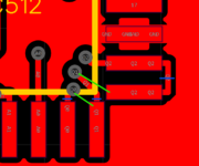 | |
Posted by: jajan547 on 2022-03-22 22:18:34Not easily. See the below image, you would have to cut the traces at the blue lines and bodge the green connections. Possible if you have a steady hand and patience I suppose.I’ll give this a shot, see how it goes. | |
| Posted by: elemenoh on 2022-03-23 14:15:47 I was able to mod the board as @SuperSVGA instructed and it did indeed work! Here's how I went about it. 1. Cut the traces as advised above and tested for continuity 2. Scraped the mask off of the affected vias 3. Placed 40AWG enameled wire into place and secured it with kapton tape 4. Soldered the socket, starting with the bodges 5. Trimmed off the excess with a hobby knife Note I did the above under a microscope. This would be a lot harder without one. It was a little fussy to do, but came out fine. Reworking the already built boards will be a bit more of a challenge because the sockets need to be removed first. 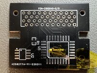 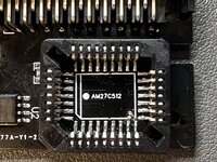 | |
| Posted by: elemenoh on 2022-03-23 17:06:38 Here's a reworked cartridge. The PLCC socket was a PITA to remove but did eventually let go. The main fallout was that a couple areas lost a bit of solder mask. This is what I did to get the socket off: 1) Sopped up as much solder with wick as possible. 2) Placed a hobby knife on the side with U2, using that as a fulcrum. 3) Heated the pins on that side until there was enough space to fit a small flathead screwdriver where the knife was. 4) Worked from left to right heating up pins to create a larger and larger wedge and eventually removed the connector. Rework of the board itself was identical to the previous post. This one tested fine after rework too. 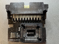 | |
Posted by: jajan547 on 2022-03-23 18:29:55Here's a reworked cartridge. The PLCC socket was a PITA to remove but did eventually let go. The main fallout was that a couple areas lost a bit of solder mask.Actually turned out quite nice, looks great @elemenoh. | |
| Posted by: SuperSVGA on 2022-03-24 02:13:52 Here's the fixed 512Kbit boards attached. My 1Mbit panels finally arrived. Next time I'm making smaller panels... 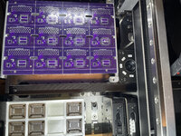 | |
Posted by: jajan547 on 2022-03-24 03:52:28Here's the fixed 512Kbit boards attached.Thanks @SuperSVGA I have organized the project and this file should be fully up to date with everything broken down into clear sections. | |
| Posted by: jajan547 on 2022-06-19 23:41:06 Please use this newest folder it's much easier and simpler to follow. | |
| Posted by: jajan547 on 2022-06-21 23:58:29 Forgot to add the updated Gerber fix for the 512k board both through hole and SMD have been fixed and are in this 2.1 Folder. Thank You To @pocketscience for the catch. | |
| Posted by: sarnau on 2023-02-08 12:09:15 FYI: I am currently looking into the firmware for the TechStep and based on that I add a few potentially interesting things:
| |
| < 9 |