68kMLA Classic Interface
This is a version of the 68kMLA forums for viewing on your favorite old mac. Visitors on modern platforms may prefer the main site.
| Click here to select a new forum. | |
| Reverse Engineering the Macintosh SE PCB & Custom Chips for 1:1 reproduction | |
Posted by: quorten on 2020-08-08 09:11:48I got all excited....plugged it in and...the PSU is dead in my SE chassis 🙁So close... I have to say I have high hopes about this. Relating to the previous discussion about the BBU pinout, it looks like it's all correct on the actual board design, Sprint Layout's misclassification of MBRAM and ROW2 was due to the fact that these are connected to pull-up resistors. Also, another note, I did find the SE PDS pinout and verified it was correct in my retrace of the schematic (one rename but otherwise good). | |
Posted by: Trash80toHP_Mini on 2020-08-08 12:48:46Sure, here on 68kMLA we all know it by its much more affectionate name, the PRAM battery, but nothing quite completes the experience of removing and replacing those beasties without the unapologetic reference designator to assign an ID number to yet another nameless battery.Is there a universal symbol for NO MAXELL for the silk screen layer? edit: on a serious note, really diggin' the progress you're making on this! :approve: | |
Posted by: techknight on 2020-08-09 21:28:15I got all excited....plugged it in and...the PSU is dead in my SE chassis 🙁Thats one hell of a cliffhanger 😛 BTW, you sure your logic board doesnt have a short on one of the rails, keeping the SMPS from starting up? | |
| Posted by: Kai Robinson on 2020-08-09 21:31:21 There's 0v reading on the output of the PSU for anything - I think its the power switch thats broken, seeing as there was a fizzing noise coming from it... | |
| Posted by: Kai Robinson on 2020-08-10 04:02:26 BTW - this is the finished board, i was so busy doing it, i forgot to post it 😀 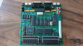 | |
| Posted by: CC_333 on 2020-08-10 12:46:59 Aside from the fact that everything is socketed and the metal frame around the ports is missing, I can't tell that it isn't a genuine SE Logic Board! But does it work? I guess you'll have to get your PSU working first before you can find out.... c | |
| Posted by: rplacd on 2020-08-10 12:51:47 ...holding my breath while that gets sorted out! If this works I'm definitely celebrating. | |
| Posted by: quorten on 2020-08-10 14:59:01 Yes, yes, loaded up with 4 MB of RAM. Relating to the idea of a replacement BBU, unfortunately it's almost, not, possible. We'd need like 74 I/O pins but best I'm seeing is FPGAs with 72 I/O in the 84-PLCC layout. (The obsolete products with 74 I/O are there to taunt me.) But hey, if we assume we don't need the two RAM config pins because everyone uses 4 MB, that would get us right down to 72 I/O pins. Unfortunately, the FPGAs still don't have a compatible I/O pinout, but a circuit board modification could take care that. Sure it's an interesting idea to think about, but yeah, probably more practical to polish up a solid implementation of the replacement RTC chip. | |
| Posted by: Kai Robinson on 2020-08-10 18:29:08 To be fair - there's no reason you can't use an FPGA with more pins than the PLCC layout - you can just not use the PLCC socket and use a standard BGA or TQFP part - like the ReAGNUS: https://www.exxoshost.co.uk/forum/viewtopic.php?t=2828 Also - the chips that should probably be concentrated on first, would be the ADB Chip (the PIC16CR54) and the GLU logic chip (PAL16L8). I have the equations but the OE list is insane... | |
| Posted by: Kai Robinson on 2020-08-10 18:33:30 Name HAL16L8; PartNo ; Date 2020-07-13; Revision 0.1a; Designer Kai Robinson; Company ; Assembly ; Location United Kingdom; Device g16v8a; /* Dedicated input pins */ pin 1 = I0; pin 2 = PB6; pin 3 = IRQ; pin 4 = WRDATA; pin 5 = ENBL1; pin 6 = PA4; pin 7 = CLK; pin 8 = PA3; pin 9 = RTxCB; pin 11 = OE; /* Programmable output pins */ pin 12 = RTxCA; pin 13 = OutA; pin 14 = IPL0; pin 15 = ENABLE_L; pin 16 = ENABLE_U; pin 17 = FLOPPY_WR; pin 18 = B6; pin 19 = FCLK; /* Output equations */ !FCLK = CLK & !OE; B6 = 'b'1; !FLOPPY_WR = WRDATA; !ENABLE_U = !ENBL1 & !PA4; !ENABLE_L = !ENBL1 & PA4; !IPL0 = !PB6 & IRQ; OutA = 'b'1; !RTxCA = !PA3 & !RTxCB & !OutA # PA3 & !RTxCB & !OutA # !PA3 & RTxCB & !OutA # PA3 & !RTxCB & OutA; That's what i pulled out of the GLU so far...makes sense, but the OE is a MESS. There must be a way to reduce them, but WinCUPL just crashes constantly. | |
| Posted by: Bolle on 2020-08-10 18:39:20 How did you figure them out? Just read the chip like a ROM and compiled the truth table back into equations? That would still leave you without the OE table though and it sounds like you have that one as well just in non-reduced form. Or was the chip actually not secured and you were able to read it with a compatible programmer? | |
| Posted by: Kai Robinson on 2020-08-10 18:43:32 Yeah - using an adapter you can read them as if they were a 27C020 ROM  | |
| Posted by: Kai Robinson on 2020-08-10 18:46:50 And here comes the OE equations... It opens fine in Notepad++ but yeah, you can see they're...nutty. View attachment glu_(1).txt | |
| Posted by: Kai Robinson on 2020-08-10 18:48:17 So yeah - you can read the contents as a .bin file while you tell the minipro 'yes, it's totally a rom', and then you parse it using the PAL analysis tool here: https://web.archive.org/web/20160124105239/http://dreamjam.co.uk/emuviews/pal/index.html | |
| Posted by: techknight on 2020-08-10 22:03:46 Yea I did this very same thing with different types of hardware that utilized combinational PALs. But the tools I used were very different, I used a tool that I made that converts the bin to a specific list of inputs and output states. As well as running it through a Python script that converts it back into primary logic. ive learned that these analyzers have issues dealing with inverted states. so if you inverted the OE, I bet it would clean that mess up. | |
| Posted by: Kai Robinson on 2020-08-10 23:27:46 Hmm - want to take a crack at the .bin i extracted? 🙂 | |
Posted by: Trash80toHP_Mini on 2020-08-11 00:29:42BTW - this is the finished board, i was so busy doing it, i forgot to post it 😀It's amazing! So glad you opted high reliability machine pin sockets, they're a beautiful touch aesthetically. | |
| Posted by: Kai Robinson on 2020-08-11 00:45:22 For salvaged parts - Dual Wipe probably make more sense, but for stuff that was socketed already, like the ROMs, definitely turned pin all the way! | |
| Posted by: Trash80toHP_Mini on 2020-08-11 01:19:46 I wonder if that would be true of desoldered IC legs? They have some vertical play built into the interface and the machined sockets might take a better bite out of desoldered pins. Dunno, interesting question. | |
| Posted by: quorten on 2020-08-11 11:18:28 A bit of a common sense check on *IPL0 on the GLU, since we also have the BBU connecting to *IPL0 via a +5V pull-up resistor, this value should only ever be high-impedance or GND, correct? If so, that common sense can certainly take a chunk out of the complexity of the OE equations. That just leaves FCLK.oe as the exceedingly complex OE equation to be dealt with. | |
| < 8 > |