68kMLA Classic Interface
This is a version of the 68kMLA forums for viewing on your favorite old mac. Visitors on modern platforms may prefer the main site.
| Click here to select a new forum. | |
| Reverse Engineering the Macintosh LC III Logicboard | |
| Posted by: mmu_man on 2021-10-09 17:51:46 Looks like you'll have to file the 96-pin one and cut into a 21-pin to get the 18-pin extension… Maybe a hot-wire would work for that. | |
| Posted by: LightBulbFun on 2021-10-10 18:49:32 its very awesome to see the home made LCIII board is finally working/booting 🙂 it really has been awesome to see all the reverse engineering going on here, some proper hard work by some very skilled people! I look forward to further progress and seeing what else gets done in the future 🙂 | |
| Posted by: joshc on 2021-10-11 01:28:00 Somehow I missed the last few updates on this. It is looking amazing! | |
| Posted by: mmu_man on 2021-11-23 18:44:09 Do you plan on publishing the files someday? Along with some netlist RE it would be useful in OpenBoardView for troubleshooting existing boards… | |
Posted by: mmu_man on 2021-11-24 03:37:05I am vaguely aware someone is working on a project to convert sprint layout files into KiCad layoutsDo you recall who that was? I fount this attempt at REing their format but it's not finished. I was looking into adding import for OpenBoardView… | |
Posted by: max1zzz on 2021-11-25 01:10:36Do you plan on publishing the files someday? Along with some netlist RE it would be useful in OpenBoardView for troubleshooting existing boards…Yes, Once the board has been finalized (and hopefully a few sold to recoup my costs) the layout files will be published Do you recall who that was?I don't i'm afraid, it was a very breif discuassion I saw on the RetroTinkering discord server some months ago | |
Posted by: trag on 2021-11-25 02:57:39Looks like you'll have to file the 96-pin one and cut into a 21-pin to get the 18-pin extension… Maybe a hot-wire would work for that. Perhaps a Dremel-type tool on a mount with a "diamond" cutting wheel? I've used that set up to separate paired 30-pin SIMM sockets. | |
| Posted by: Trash80toHP_Mini on 2021-11-26 01:22:13 Easiest way to do it is with a razor saw from X-Acto or preferably, a pull stroke fine cutting Japanese type flush cut/dovetailing saw. Three 96pin slots make two 130pin slots. When buying "96" position slots, make sure all 96 pins are implemented. It's easy to wind up with only two rows/64 pins on useless connectors. | |
| Posted by: djhaloeight on 2021-12-18 22:09:31 Read thru this thread in full tonight. Max, you’re a genius mad scientist! | |
| Posted by: mmu_man on 2022-01-01 09:51:31 Did you look at the DIN connector yet? There are 3x16 ones on aliexpress that might be cut in two halves I suppose (one requiring some more filing on the plastic key). It should be possible to make a small PCB as cutting rig with marks on the silk screen. | |
| Posted by: max1zzz on 2022-01-01 10:26:57 I haven't looked at it much yet, I did purchase some 120pin connectors wit the intention of cutting slot out of them but your method seems a little simpler I Need to order some stuff from aliexpress tonight so I'll order some of those and give it a go! | |
| Posted by: marciot on 2022-03-16 13:47:01 @max1zzz: This is amazing work! I'd like to ask you a favor, would you be able to share a JPG or PDF of the board layers for this lower section of the LC III motherboard near the internal HD connector? This unfortunate board underwent a Chernobyl-type situation with the battery that obliterated the traces and vias in this portion of the board. I would like to see if I can repair it by running some wires, but the board is so destroyed in this area that I can't make out where the traces used to go. 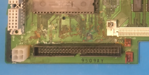 | |
| Posted by: max1zzz on 2022-03-16 14:56:19 @marciot Of course 🙂 I have just uploaded the trace layouts to: https://github.com/max234252/Macintosh_LCIII-Reloaded/tree/main/Copper I'm currently in the progress of preparing the project for a "release" so the board layout etc will be uploaded to github soon too 🙂 | |
| Posted by: marciot on 2022-03-16 15:53:27 @max1zzz: Thanks! This will help prove or disprove some of my theories! So I've been looking at the schematics from Bomarc and found out that the PDS slot is like a giant breadboard with all the important signals. How convenient! I've been using my multimeter and have just finished buzzing out all the data lines from the ROM chips to the PDS slot. All except one were good, so I am pleased that at this point that most of the data lines from the ROM seem to be okay, which was my primary concern. I'm betting trace damage will be clustered in the conduits to U35/36/37, which at this point I do not know the purpose of, although I am guessing they multiplex the address lines, so they must be fairly important to get right. | |
| Posted by: mmu_man on 2022-03-16 16:56:34 The PDS slot pinout is in the LC-III Developer Note btw, page 30 (well, 40 in the PDF). | |
| Posted by: marciot on 2022-03-16 17:13:06 Thank you, guys! I've just done the first pass of figuring out where all the likely broken traces go and fixing this guy is gonna be a doozy -- some 35 to 40 different bypass wires will be needed, at least! This board is gonna have to look like one of those wire-wrapped computers from the 60s before it ever boots again... 😁 | |
| Posted by: cheesestraws on 2022-03-16 17:28:43 Gives it character! | |
| Posted by: John_A on 2022-03-17 13:31:57 I’m late to the party and you may have covered this already. But where do you get the components to populate these new mother boards? New? Nos? Salvaged parts? A combination? | |
Posted by: max1zzz on 2022-03-17 15:03:36I’m late to the party and you may have covered this already. But where do you get the components to populate these new mother boards? New? Nos? Salvaged parts? A combination?I'll always be a combination or purely salvaged as these boards contain a number of custom IC's (The memory controller, clock chip, CULTDAC, DFAC and EGRET) so you'll always need a donor board for these. Initially when building these I was always replacing the passives with new but in the end I actually found it is much quicker and easier to just move all the passives over form the donor boards | |
| Posted by: max1zzz on 2022-03-17 16:33:05 The board layout, Gerbers, Copper layout and board scans are now available! GitHub - max234252/Macintosh_LCIII-Reloaded: 1:1 Reproduction of the Macintosh LC III PCB1:1 Reproduction of the Macintosh LC III PCB. Contribute to max234252/Macintosh_LCIII-Reloaded development by creating an account on GitHub.
 github.com
As with the LCI board this is provided under a non-commercial license however if you provide repair services and want to provide these boards (Or want to use them for any other commercial purpose) please contact me | |
| < 6 > |