68kMLA Classic Interface
This is a version of the 68kMLA forums for viewing on your favorite old mac. Visitors on modern platforms may prefer the main site.
| Click here to select a new forum. | |
| Macintosh Portable SRAM card: Schematics available? | |
Posted by: Gorgonops on 2020-04-30 14:57:35That's a rather big project FWIW, at least everything on it other than the EMS mapper (and the replacement of other decoding logic with GALs) has already been tested before. Here's a picture of my first prototypes running. (The three PCBs piggybacked on top of the Tandy motherboard.) 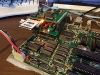 | |
| Posted by: Gorgonops on 2020-04-30 17:10:37 ... per that last picture and what I said about caps with their leads "pre-splayed": if you look at the top card in that stack you can see how the disks in the row next to the vertically oriented chips are sitting kind of awkwardly sidewise? Those are a slightly different value of cap buffering RS232 serial lines. They're the same diameter (or even smaller than) some of the disks I'm using for the power line decoupling but they have this weird wide-squat shape to the leads. Don't buy caps like that. 😉 (Wasn't the end of the world, I just tilted the whole cap over sidewise and it fit fine, but if your board were really dense it could be a problem.) | |
| Posted by: Stephen_Usher on 2020-05-01 08:18:03 That's a mighty tower you have there! Is that a TRS-80 CoCo? | |
| Posted by: LaPorta on 2020-05-01 09:24:07 Two questions from a decidedly hardware-dumb individual: 1. Does that card design work? 2. When can I get one for my portable? | |
Posted by: Gorgonops on 2020-05-01 10:32:53That's a mighty tower you have there! It's the motherboard from a Tandy 1000 HX. Those and their sister machine the 1000 EX are really oddball PC compatibles that are packaged in "computer in a keyboard" format that looks kind of like a gigantic cross between a Color Computer III and an Apple IIc. The motivation to start building cards was getting a bare 1000 EX last year; these machines have only 256k on the motherboard and they use a proprietary expansion card format that involves a single 62 pin header on the motherboard instead of a standard ISA slot. (They called the resulting cards "Plus" boards.) The bizarre way Tandy set it up means either you can only have one "parasite" card (my EX came with a modem in the slot), which leaves you stuck at 256k forever, or they sold you a special memory card that had two different-height headers splayed out so you could stack two additional parasite cards on top. The cards in my stack there are a memory card that replicates the staggered stacking connectors at the bottom, an IDE/Compact Flash adapter card derivative of this design, and a dual-port serial card. My new card has *all* the functions on one board, but I'm retaining the stacking connectors so I can keep going with a network card or, I dunno, plug that useless 1200 baud modem that came with the machine back in. I made some boring-as-heck rambling videos about the Tandy 1000 saga as of late December. Obviously I haven't figured out what to do with the youtube channel since. Honestly I don't know why Tandy didn't use either a conventional ISA riser or a straight-up stack-through header design like PC-104. There's a lot weird about these machines, which makes them kind of awesome. | |
| Posted by: Stephen_Usher on 2020-05-04 14:59:31 Well, the PCB design is off to PCBWayyyy... (Sorry, I've been watching far too many "Retro Recipes" videos on YouTube.) Hopefully this will be what it looks like (tall, red capacitors replaced by yellow blobs). 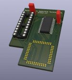 | |
| Posted by: Gorgonops on 2020-05-04 15:16:06 Woot. Soon we'll find out just how wrong my GAL code is. 😉 My first board using GALs is, according to JLCPCB, waiting for DHL to pick it up. I've tested the GAL code for that using my handy-dandy Arduino count-a-matic rig and it looks good, so, well, my guess is if it doesn't work it's more likely to be because the sheer crazy density I tried to squeeze onto a two-layer through-hole board was a bridge too far. | |
| Posted by: techknight on 2020-05-05 10:04:23 hell yall gone this far, you could just simply make a whole new RAM card with that stuff embedded on it. 🙂 | |
| Posted by: Stephen_Usher on 2020-05-06 07:23:25 I de-soldered the "Dunkirk" chip today and replaced it with a socket. Now I have an issue of mechanical interference between the chip socket and the RAM board socket I'm going to have to look into. I had sanded the socket down a bit because I thought that this may be an issue but it's not enough. I may have to trim the plastic. | |
| Posted by: Gorgonops on 2020-05-06 10:52:14 Ugh. Looking at a picture of the Portable's motherboard I'm kind of concerned whether you're going to have enough clearance for that socket adapter and the board before you run into the PDS slot. With the "Dunkirk" nestled low in the corner like that there's all sorts of room for interference there. | |
Posted by: Gorgonops on 2020-05-06 11:02:13hell yall gone this far, you could just simply make a whole new RAM card with that stuff embedded on it. 🙂That's what I said. 😉 (Technically Apple wants you to buffer everything so a new-build board *should* have a row of '244s and '245s on it in addition to the GAL. But, hey, if you used *one* of those CY62167G-45ZXI 2MB chips wired straight to the bus then the loading should be about the same so, yeah, use one of those and the PLD and, bam, 2MB memory card. Or live dangerously and use two of the cypress chips for 4 meg.) | |
| Posted by: techknight on 2020-05-06 11:07:46 or, simply use what I created, get 8MB, and it works perfectly 🙂 | |
| Posted by: Gorgonops on 2020-05-06 11:59:19 Well, yeah, there's certainly that. I was assuming "make it yourself because education" was also a factor. 😉 Also was just pointing out that *theoretically* if you bent the rules you probably could make a functional memory card in the same number of chips as that adapter card. (IE, a RAM chip wired straight to the bus and a GAL or whatever to decode it.) Unfortunately it looks like 2MB is about the absolute limit for 5v compatible SRAM chips... except *maybe* some in BGA packages? (Thought I *might* have seen a 32Mbit/4MB one while looking for parts options a while back that was 5v but only came in BGA.) | |
| Posted by: Trash80toHP_Mini on 2020-05-06 17:48:43 Are four layer boards all that much more expensive in the sizes you need? There's also the ugly route: pinning a pair of two layer boards together wherever needed with headers to be clipped off with the plastic spacer width between the boards. header/socket connections until you verify overall function, quad check the inner "layers" and then smoosh 'em together. [}🙂] | |
Posted by: Stephen_Usher on 2020-05-07 14:10:59Ugh.There's enough clearance as long as I don't try to insert a PDS card. I don't have one for the slot anyway. The board itself has a cut-out for the connector space. the issue is the lack of clearance between the socket end and the PLCC socket. That can be fixed in one way or another. | |
Posted by: Stephen_Usher on 2020-05-07 14:13:16Are four layer boards all that much more expensive in the sizes you need? There's also the ugly route: pinning a pair of two layer boards together wherever needed with headers to be clipped off with the plastic spacer width between the boards. header/socket connections until you verify overall function, quad check the inner "layers" and then smoosh 'em together. [}🙂] Looking at PCBway, 4 layer boards are about 5 times the price of 2 layer and have a lead time of a week rather than 24 hours. I did try my board routed on a 4 layer board but Freerouting didn't do a very good job especially as it didn't seem to understand a ground plane. | |
Posted by: Gorgonops on 2020-05-07 15:16:35did try my board routed on a 4 layer board but Freerouting didn't do a very good job especially as it didn't seem to understand a ground plane.I'm not sure what benefit more layers would be, it's not like it's that complicated of a board. Most of the real estate is taken up by the physical chips. | |
Posted by: Stephen_Usher on 2020-05-08 02:42:37I'm not sure what benefit more layers would be, it's not like it's that complicated of a board. Most of the real estate is taken up by the physical chips.Technically, having a complete ground plain on both sides of the board with the active traces on top dampens noise. To be honest I only did it as a "I wonder what would happen if" experiment. I never contemplated actually doing it. | |
| Posted by: Gorgonops on 2020-05-08 08:51:13 If you were making something that ran at... maybe a few dozen MHz or faster you might need that but it does seem like a stretch here. | |
| Posted by: Stephen_Usher on 2020-05-11 03:57:46 The new PCBs have arrived. I'm not sure when I'll get the time to make one up though. 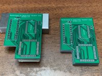 | |
| < 5 > |