68kMLA Classic Interface
This is a version of the 68kMLA forums for viewing on your favorite old mac. Visitors on modern platforms may prefer the main site.
| Click here to select a new forum. | |
| Reverse Engineering the Macintosh SE PCB & Custom Chips for 1:1 reproduction | |
| Posted by: Kai Robinson on 2021-01-01 03:06:46 Just attaching this for reference later on. 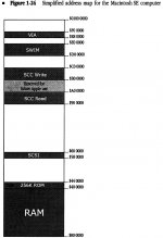 | |
| Posted by: Kai Robinson on 2021-01-01 05:10:57 BTW - anyone invested in this project such as @techknight, @maceffects, @quorten, @asicsolutions, @cheesestraws and anyone who has been sent a rev 1.4c board - please join the Retro Tinkering Discord: https://discord.gg/8dJxmF8Tzh - easier to chat in there about things to save this thread from getting too cluttered! 🙂 | |
Posted by: techknight on 2021-01-01 05:48:45BTW - anyone invested in this project such as @techknight, @maceffects, @quorten, @asicsolutions, @cheesestraws and anyone who has been sent a rev 1.4c board - please join the Retro Tinkering Discord: https://discord.gg/8dJxmF8Tzh - easier to chat in there about things to save this thread from getting too cluttered! 🙂 Seems like its more Amiga than anything else. Amiga really isnt my thing. | |
| Posted by: Kai Robinson on 2021-01-01 06:10:15 There's the mac specific channels for the SE and SE/30 - more rooms created as needed. | |
| Posted by: CharlesT on 2021-01-01 06:55:06 Is anyone familiar with the bootloading process following reset? The 68000 data sheet shows going to address 0 following reset, which is RAM, but ROM, which presumably is where the loader resides, starts at 0x40,000. And Kai, most of the 68K signals are available on the PDS slot, so populating the desired pin sockets with a hand full of square post pins should provide a good connection point for the LSA pods. | |
| Posted by: quorten on 2021-01-01 06:58:10 @CharlesT The BBU has an internal soft switch for the ROM Overlay signal, which remaps the ROM to address zero on reset, and the RAM is likewise remapped. It is disabled on the first regular ROM access. | |
| Posted by: techknight on 2021-01-04 07:48:43 Once upon a time, Motorola recommended a design that I believe was a counter for overlay. so after so many clock cycles from RESET, it would switch the ROM back. | |
| Posted by: ScutBoy on 2021-01-04 11:19:27 I've retrieved the BrainStorm SE and will send the logic board and bits off to Maceffects. here's an album of pictures. Sorry for the link out, but the gallery upload here was flakey. I'll try to get them "locally" here when I can. https://flic.kr/s/aHsmTrg1ko | |
| Posted by: Kai Robinson on 2021-01-04 12:01:13 Hmm those EN64K's...they could be 6264 SRAM? Either that, or bus transceivers - they seem to be connected to the data bus...? | |
Posted by: demik on 2021-01-04 12:12:00Hmm those EN64K's...they could be 6264 SRAM? Either that, or bus transceivers - they seem to be connected to the data bus...? Could be ! Bottom one is connected to D0😀7 and top one is connected to D8😀15 Looks like the 6264 SRAM pins indeed : https://en.wikipedia.org/wiki/6264 | |
| Posted by: maceffects on 2021-01-04 16:47:48 @ScutBoy thank you! This appears to be SMD mounting. I think it can be converted to through hole DIPs. But I may keep it the same way. DIP and PLCC processors are available. @Kai Robinson I was initially worried that these were some kind of custom logic chip but appear too small for that and do share the same package as the SRAM. What is your level of confidence that these are SRAM? The only contingency that would remain is simply the custom BBU. I found a company in China that can get the equations from the chip by various processes but it will exceed $600 (their minimum price - and it’s destructive). I’m hoping once the breakout comes in, I can assembly it and send it to @asicsolutions for review. | |
| Posted by: Kai Robinson on 2021-01-05 01:13:03 @maceffects For the BBU - i'd be willing to stump up a spare BBU - FOR THE CAUSE. As well as the $. I'm due to cash in some stock options again this year to put down a 20% house deposit - i can spare $1000 for this. Regarding the plug in board - tbh, i'd map out the schematic of it - then i'll make a board design based on it - with SOIC parts, still, but with a SMD PLCC socket for the CPU. For SOIC - you can hand solder these parts, no need to use hot air. | |
Posted by: maceffects on 2021-01-05 08:44:24@maceffects For the BBU - i'd be willing to stump up a spare BBU - FOR THE CAUSE. As well as the $. I'm due to cash in some stock options again this year to put down a 20% house deposit - i can spare $1000 for this. I'm going to see what we can do without having to spend any cash now. I am really hoping to be able to clone the Brainstorm BBU rather than the stock BBU as it will be something we can learn from and be able to possibly make better than stock BBU without people needing the 16mhz PDS upgrade part as well. I'm really mainly concerned that I don't want to waste the BBU/PDS with destructive reverse engineering as I'd like to return it to ScutBoy in the same condition. However, if i KNEW with a high level of certainty that China would be able to provide us the info needed to reverse engineering, it might not be an issue as I can simply make new parts for him. Destructive reverse engineering is a last resort, however, if you want to do a stock one that would be helpful too. I don't want to spend $600+ on making a stock BBU design. But maybe either can give up their secrets and allow us to know what to do. | |
| Posted by: ScutBoy on 2021-01-05 09:34:44 Wouldn't kill me if we needed a destructive teardown of the Brainstorm BBU, but it would be a bonus if we could preserve the original. So - don't rule it out if that's what it comes to. | |
Posted by: SlickClick on 2021-01-05 12:10:58@Kai Robinson they look lovely. Excuse my potential ignorance, but isn’t the SE limited to 1mb SIMMs? And if I recall many Macs of this era didn’t like 3 chip memory SIMMs. If you think we have a way to allow more memory, I’d be very keen on learning more.Actually on Paper the 68000 supports up to 16Mb of RAM... I suspect because of the limited amount of Bus Lines to/from the SIMM Slots is the Limiting Factor for the Base Model SE; that and that the ROM would need Modification to Recognize/Access Limits Higher than 4Mb... IDK; but it is possible that there is a Physical Hardware Block or Value/Signal sent/set to the CPU; for instance the difference in cutting the resistor to allow for 1Mb SIMMs over 256k SIMMs... I suspect that it might be possible to make some RAM chips that would Max out the RAM abilities of the CPU... Technically you can make Half Meg (512k) chips too... For Instance a 1.5Mb SIMM might be a fair starting place since you have a 3-Chip module setup; so if you put 3-512k RAM chips on it, it might not be too much additional memory range to utilize... I have a feeling that with a properly designed SIMM a 2Mb SIMM could be made/used; possibly even a 3Mb SIMM which since you have 3-chip modules slap on 3-1Meg chips and see what happens... I believe that 12Mb is Obtainable... | |
| Posted by: maceffects on 2021-01-05 12:14:41 @SlickClick interesting hypothesis. Certainly, outside of my domain but I would love to see a SE be able to get 12mb of memory especially coupled with 16mhz 68000 processor. I'll leave that to the experts, however. | |
| Posted by: Kai Robinson on 2021-01-05 12:56:48 Well those 3 chip modules are 2 actual RAM and 1 is the 1-bit Parity RAM chip, which isn't used on macs (except TEMPEST and DoJ/DoD specific purchased Macs). It's more a limit of the BBU - not enough pins for outputting all the RAM address lines. Plus in 1987 - 4MB was considered a flight of fancy for most, so it wasn't really a concern. Like i mentioned earlier - it may be possible for whatever BBU replacement to address the additional lines, using extra pins on whatever PCB fits in there, and it'd be trivial to add the connection on the Logic board side of things. | |
| Posted by: Kai Robinson on 2021-01-05 13:14:20 I think we're far enough in, by now - that it's about time i posted the Sprint Layout file and the high resolution scans used for Sprint, for all and sundry. This is the current 1.4d revision, with the fixed A5 line - IT IS NOT GUARANTEED TO WORK (not yet!), and if the board is fine, and it's verified working, then i'll post that revision (if one is needed). This is, after all, an open-source, community driven project, done for the good of the community. When this project produces working boards - i'll still sell them - probably for around £20 to £25 per PCB, to anyone that wants one, but feel free to make Gerbers of your own, modify the design to your hearts content...but please leave the silkscreen credits alone, is all i ask 🙂 View attachment Macintosh SE Project.zip | |
| Posted by: quorten on 2021-01-05 15:04:03 @maceffects It's also useful to reflect upon Brainstorm's historic business model, which was to first reverse engineer the Macintosh Plus PALs and then use that knowledge to create the Macintosh SE BBU replacement. I'd reckon that method on its own must have created pretty good results. As far as reverse engineering the Brainstorm is concerned, most of our efforts should really just be focused on analysing the software of the embedded 68k processor on the PDS. I'd guess the Brainstrom BBU is not an FPGA and has no firmware of its own and the firmware upgrade only goes toward the embedded 68k processor, but maybe it is actually used as a loader for the BBU that's just an FPGA. Well, either way, my two cents, there's nothing interesting to see by destructive reverse engineering of the Brainstorm BBU directly. | |
Posted by: SlickClick on 2021-01-05 20:08:08@maceffects It's also useful to reflect upon Brainstorm's historic business model, which was to first reverse engineer the Macintosh Plus PALs and then use that knowledge to create the Macintosh SE BBU replacement. I'd reckon that method on its own must have created pretty good results. As far as reverse engineering the Brainstorm is concerned, most of our efforts should really just be focused on analysing the software of the embedded 68k processor on the PDS. I'd guess the Brainstrom BBU is not an FPGA and has no firmware of its own and the firmware upgrade only goes toward the embedded 68k processor, but maybe it is actually used as a loader for the BBU that's just an FPGA.Technically the board/chip could be X-Ray'd... There is also tracing software these days that help trace the board lines out & identify ICs... These older machines are mostly all 2-layer PCB designs & the PDS slot is a dream as it provides direct access to the Data bus lines.... | |
| < 29 > |