68kMLA Classic Interface
This is a version of the 68kMLA forums for viewing on your favorite old mac. Visitors on modern platforms may prefer the main site.
| Click here to select a new forum. | |
| Beige G3 onboard cache | |
| Posted by: stynx on 2025-04-04 03:08:21 Gossamer's Tale The quest for onboard cache I have been looking around for hints on how to install the 2nd-level cache slot on the beige G3. There is unpopulated component, most likely a socket, that is labeled cache and is connected to the Grackle bridge. The pinout is in the schematics. Sadly, i could not find a source for the cache slot component. But i think i have found the origin of the cache socket and cache-dimm. 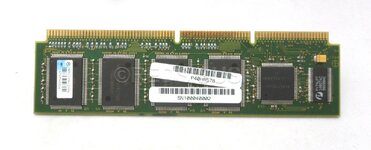 There is a cache module from the IBM RS6000 7043 p-series that would fit. It has the VCC and GND pins at the correct locations and is (at least) 66MHz capable. The cache size is 1MiB and would perfectly fit into the timeframe. The Grackle controller, the VRM and the CPU-ZIF socket are also identical to the Gossamer board. The IBM cache-socket is a bit longer and has an addition that is seemingly not used. The cache-socket also lacks the second notch, which the cache-module has. Maybe IBM had intended to use a variety of different cache modules.  Since i live in Germany, any attempt to buy a RS6000 board to get my hands on a cache-socket have failed due to enormous prices the sellers slap on for shipping ($100 for the board with CPU and cache, $700 shipping). Im still looking into getting a cache module to (maybe) manually solder it in. It would make a comparison between G3 and 604e more interesting and maybe the onboard-cache could be used with the G3? There are hints, that a 4MiB cache module from IBM has existed but maybe that's what the extension is for on the socket. | |
| Posted by: stynx on 2025-04-04 03:23:23 Here are some images of a close-up of the cache on the RS6000 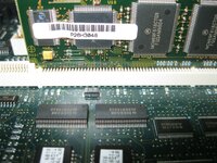 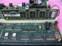 | |
| Posted by: stynx on 2025-04-04 03:35:50 Here is a PDF from Motorola about the cache module edit: The cache described in the PDF is not the same as the IBM cache. The PDF describes a 178 lead package while the IBM cache is a 182 lead package (like the Gossamer socket) 512KB and 1MB BurstRAM Secondary Cache Modules for PowerPC and PReP/CHRP Platforms | |
| Posted by: stynx on 2025-04-04 03:46:43 Here is the correct Datasheet: | |
| Posted by: stynx on 2025-04-04 03:48:02 The socket part number is Burndy ELF182JSC–3Z50 Here is a comparison between the cache module pinout and the Gossamer pinout: 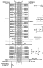 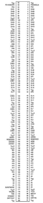 | |
Posted by: croissantking on 2025-04-04 05:47:35The RS6000 looks a bit like the unreleased Starmax 6000 board. I guess it’s no accident they’re both numbered 6000. By the way, wouldn’t a cache socket from a PM7300-9600 machine physically fit the Beige’s cache slot footprint? | |
| Posted by: Powerbase on 2025-04-04 05:55:28 I mean, they did use the same socket as the Beige/B&W G3s. That's the source of the higher clocked 604 ZIFs. Probably the leftover developments from whatever CHRP work they must have helped with, I'd assume. I've looked at the cache in those RS boards too and they 'seem' similar, but I didn't want to take the chance of frying something, if it managed to physically fit. | |
Posted by: stynx on 2025-04-04 10:30:47By the way, wouldn’t a cache socket from a PM7300-9600 machine physically fit the Beige’s cache slot footprint?No, the older cache slots are 5V while the G3 is 3.3V | |
Posted by: croissantking on 2025-04-04 10:45:19No, the older cache slots are 5V while the G3 is 3.3VAre they keyed differently? I haven’t checked. | |
Posted by: stynx on 2025-04-04 12:26:10Are they keyed differently? I haven’t checked.Yes, they are. | |
| Posted by: herd on 2025-04-04 12:30:21 Interesting, I hope you can get some parts to test. They do look like different pins/spacing than these: 68kmla.org/bb/index.php?threads/6360-6400-6500-l2-cache-modules.38450/ | |
Posted by: stynx on 2025-04-04 12:39:39Interesting, I hope you can get some parts to test. They do look like different pins/spacing than these:The cache in the G3 has 182 "pins" while PCI mac cache has 160 "pins". The G3/RS6000 cache module is a bit bigger. | |
| Posted by: Coloruser on 2025-04-05 04:36:21 Back in those prep/chrp days, gossamer and other mainboards like yellowknife or long trail etc. were designed with both 604e and 750 in mind. RS/6000 had 601 and 604 and some RS/6000 were based on CHRP. Thus, a L2 cache would be beneficial for 604e based boards. I worked with a Tatung 6000 prototype board and with 604e CPUs in its socket, a L2 was more or less mandatory. But the operation manual clearly stated that with a 750, the L3 should me removed. However, when later G4s got faster and the bus interface (601 or max bus) did not really develop further, Apple introduced L3 caches on first on some higher end G4 quicksilver/DA machines and on all MDDs to offset the gap between L1, L2 and the comparatively slow 133/167 Mhz maxbus to Ram. However, with the much slower early G3s and a thus much slower gap between CPU, L2 and Ram, the L3 might be creating more overhead than benefit. | |
| Posted by: Coloruser on 2025-04-05 04:39:47 See the Motorola Yellowknife L2 schematics…. https://www.nxp.com/docs/en/reference-manual/YKNIFEX4HW.pdf or IBM‘s long trail here: https://www.applefritter.com/files/lt_tour.pdf 160pin Cache on a Stick (Coast) module - more in line with the PCI powermacs…… | |
| Posted by: stynx on 2025-04-07 09:43:27 Interesting comparison... 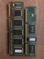 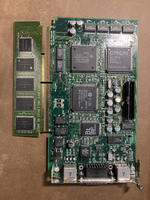 The PPC PDS slot might work as a slot-solution for the G3, even though it is possibly too tall for the G3 to close. EDIT: The Perch-Slot has the mostly the same dimensions and the cache would fit. Edit2: looks like there are some in stock here: https://www.connectorpeople.com/Connector/BURNDY/C/CEE2X91S-3Z14 | |
| Posted by: stynx on 2025-04-07 10:38:08 Mouser has a variant as well: -- correction -- It is possibly not the correct slot since it has 41-48pos while the needed slot has 42-47pos | |
Posted by: stynx on 2025-04-09 11:35:28Mouser has a variant as well: -- correction -- It is possibly not the correct slot since it has 41-48pos while the needed slot has 42-47posI have bought two slots and they fit. It is the same as the Perch slot and the same as the PPC PDS slot. I will try to solder the slot in at the weekend. Ok, i just tried fitting one of the slots into the Gossamer board. It did not fit. The number of pins is ok, the spacing is ok BUT the pin arrangement is wrong. The ins are opposite to what they should be. I have begun to "shift" the pins one pin "up" but that is much work and the amount of pins i have bent beyond repair is also too high. | |
| Posted by: stynx on 2025-04-10 13:24:20 DON'T TRY THE L3-CACHE MOD! I have soldered in the socket after painstakingly assembling it and after installing the L2-cache module.... The module released smoke and a hissing noise.... I instantly pulle the plug but the G3 would not boot without the L2 cache module, just a blank screen. I tinkered a bit around and found out that only the Rom-card was dead. That was a close one... The cache module has seemingly some pins different than the Apple slot although i had compared the VCC and GND with the Gossamer schematic. I seem to have overlooked something. | |
| Posted by: croissantking on 2025-04-10 13:27:12 Whoa! | |
| Posted by: stynx on 2025-04-10 13:46:05 Here is the damages cache module. I just had a thought: Maybe the engineers at Apple f'cked up and did the pinout on the socket wrong and never really had to correct the issue since the cache slot was never used? I have only found reserved pins in the effected area that are pulled high (3.3V). | |
| 1 > |