68kMLA Classic Interface
This is a version of the 68kMLA forums for viewing on your favorite old mac. Visitors on modern platforms may prefer the main site.
| Click here to select a new forum. | |
| Macintosh SE/30 logicboard recreation (thread revival) | |
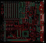
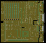
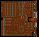
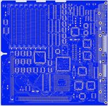
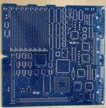
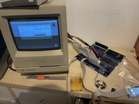
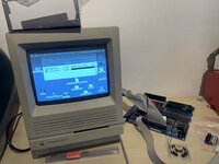
| Posted by: Bolle on 2021-11-13 11:04:02 I recently finished testing on the final (so far) working revision of the SE/30 board. Below is my initial post from before the site crash on how everything started: Just like I promised when teasing everyone in the SE logicboard thread here we go with the build-log/information exchange/everything thread on the SE/30 logicboard replacement PCB. All things on the "left to do" list had been worked out before the site crash. Just recently I found the time to finally order a batch of revision 2 boards with the SCSI blooper fixed and PLCC32 ROM sockets added. Now just look at this beauty: 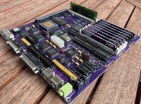 Passed all tests, no bodge wires needed and already has been running 3 days straight now without any hiccups. Board files, reverse engineered PAL files and BOM available on github: GitHub - TheRealBolle/SE30: Macintosh SE/30 logicboard recreationMacintosh SE/30 logicboard recreation. Contribute to TheRealBolle/SE30 development by creating an account on GitHub.
 github.com
Many thanks go to... @joshc for putting together the BOM @cheesestraws for supporting me with reverse engineering the PALs @Siliconinsider for making those beautiful die shots of the GLUE https://www.siliconpr0n.org/archive/doku.php?id=bercovici:apple:344s0602-a - who's going to give recreating that one a go now? 😉 @Kai Robinson for putting together pick and place files (also found in the github) and finally @GeekDot for bugging me into starting with this project in the first place and working on the (not yet working) in system ROM flashing software when using the PLCC32 ROM sockets (more on that later - probably) I'll clean up the github over the next days and add some more descriptive information. | |
| Posted by: Byte Knight on 2021-11-13 12:15:56 Looks awesome - great work!! | |
| Posted by: robin-fo on 2021-11-13 12:53:25 Brilliant work! Is there any chance to get one? | |
Posted by: Bolle on 2021-11-13 13:08:51Is there any chance to get one? Like a fully assembled one? No, not from me. You'll need a SE/30 donor board, order your own PCBs from a manufacturer of your choice with the files from the github and then assemble it on your own. | |
| Posted by: TPope on 2021-11-13 13:24:48 Looks really nice. | |
Posted by: robin-fo on 2021-11-13 13:27:31Like a fully assembled one? No, not from me. You'll need a SE/30 donor board, order your own PCBs from a manufacturer of your choice with the files from the github and then assemble it on your own.No, I mean just the board. I do have a spare SE/30 board and would be willing to populate it myself. I simply assumed you might have had to order a bunch of them from your manufacturer and now have some spare ones... | |
| Posted by: ktkm on 2021-11-13 14:02:30 Beautiful! And no batteries as far as the eye can see! I want a fully assembled one really bad, what do I need to do!? | |
Posted by: joshc on 2021-11-13 14:08:28Beautiful! And no batteries as far as the eye can see! I want a fully assembled one really bad, what do I need to do!?The gerbers and BOM are in the GitHub repo that Bolle posted. A place like https://jlcpcb.com/ can be used to order the PCB using the gerber files. The BOM tells you what parts you'll need to order. But you need a donor SE/30 board to pull the custom ICs from to build your board. @joshc for putting together the BOMThank you, it was a fairly long project doing that and I hope it proves useful for people. I will make further updates to it to make it even easier to use. Now just look at this beauty:It certainly is beautiful, everything needs to be purple from now on! 😀 | |
| Posted by: max1zzz on 2021-11-13 14:32:40 Ooh very pretty 🙂 Kinda wish I hadn't just sent off a order to JLCPCB, Guess i'll have to add some of these to my next order 🙂 | |
Posted by: Trash80toHP_Mini on 2021-11-13 15:06:33It certainly is beautiful, everything needs to be purple from now on!Black shows off the traces and silk screen layer to better effect. Neutral black would also tie together BolleWerke-BLUE in PDS, PurpleSIMM therin and BMOW/dougg3 RED in the ROM Slot. | |
| Posted by: nickpunt on 2021-11-13 15:09:30 Congrats @Bolle this is a big achievement! Great for replacements and a solid foundation for next level SE/30 hacking. | |
| Posted by: CC_333 on 2021-11-13 22:40:42 Oooo! I really want one of these, but I don't know how to justify it because I have a fully functional original that I'm happy with. Now I feel like I have to intentionally find a battery-bombed board so I can fix it with one of these new ones! c | |
| Posted by: Daniël on 2021-11-14 03:33:39 Fantastic work! I have a couple of grotty SE/30 boards, so a couple of these are in my future. That luscious purple is probably the pick for me, will go nicely with the blue BolleMac Carrera040 and PDS passthrough adapter 🙂 | |
| Posted by: cheesestraws on 2021-11-14 06:36:19 This has been a fun project to follow along with (at a considerable distance behind). Great stuff. | |
| Posted by: pax on 2021-11-14 07:27:10 Spectacular achievement, congratulations to you @Bolle and to us in the community! | |
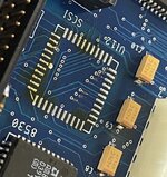
Posted by: GeekDot on 2021-11-14 08:33:08[...] and finally @GeekDot for bugging me into starting with this project in the first place and working on the (not yet working) in system ROM flashing software when using the PLCC32 ROM sockets (more on that later - probably)Oh dang, you're right... need to resume that. I dived way too deep into the Apple IIgs universe. So I need to populate my (rev.1) soon to have an "in vivo" test-bench instead those dreaded 'try now' sessions 😉 Also I noticed that the orientation of the diodes D4-D19 is wrong in the provided CPL file (at least for the JLC lib) - They're all at 0° and need to be at 270°. Here's a quick look (I corrected D14/D16 as an example): 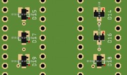 ...and for those, seriously considering to have that beauty made and use their SMT service (I recommend the back-side): It'll be $120US (~105€) plus shipping 😵 Just sayin' Beyond that: Love you, Bolle! Always did! 😆 | |
| Posted by: aeberbach on 2021-11-14 15:22:18 Congratulations to everyone involved, that's great work. | |
| Posted by: Daniël on 2021-11-15 00:06:45 I was looking at adding to a JLCPCB order, and noticed it asked me for the layer order (which layer is the top layer, which on the top-middle layer, which the bottom-middle layer, which the bottom layer). I think I know what files should be picked, but I figured I ask here what should be picked there, so others with the same question can read it here 🙂 | |
Posted by: GeekDot on 2021-11-15 00:15:30I was looking at adding to a JLCPCB order, and noticed it asked me for the layer order (which layer is the top layer, which on the top-middle layer, which the bottom-middle layer, which the bottom layer). I think I know what files should be picked, but I figured I ask here what should be picked there, so others with the same question can read it here 🙂The order of the layers is automatically defined by the gerber files - so it seems that something went wrong during your order process (create a zip file from the "board files" folder and upload that). But as long as the top- and bottom-layers are on the outside, everything else belongs into the esoteric field of discussion (at least for 4 layer designs). Also the provided BOM/CPL files are meant for the back-side only. NB: If you choose their SMT service you can only choose green as PCB color! No fancy purple 😉 | |
Posted by: Daniël on 2021-11-15 00:28:54The order of the layers is automatically defined by the gerber files - so it seems that something went wrong during your order process (create a zip file from the "board files" folder and upload that). I downloaded the entire GitHub as a ZIP, then removed all files and folders inside other than the board files folder. Just to be sure, I downloaded the GitHub again, but this time extracted the board files folder and rezipped that. I still get asked for the layer stackup, so I'm not sure if this is required to be filled in? I've not ordered boards more than two layers before, so this might be more obvious for others. 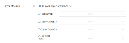 | |
| 1 > |